- 您現(xiàn)在的位置:買賣IC網(wǎng) > PDF目錄296642 > MT46V128M4P-75L:C 128M X 4 DDR DRAM, 0.75 ns, PDSO66 PDF資料下載
參數(shù)資料
| 型號(hào): | MT46V128M4P-75L:C |
| 元件分類: | DRAM |
| 英文描述: | 128M X 4 DDR DRAM, 0.75 ns, PDSO66 |
| 封裝: | 0.400 INCH, LEAD FREE, PLASTIC, TSOP-66 |
| 文件頁數(shù): | 53/94頁 |
| 文件大?。?/td> | 4179K |
第1頁第2頁第3頁第4頁第5頁第6頁第7頁第8頁第9頁第10頁第11頁第12頁第13頁第14頁第15頁第16頁第17頁第18頁第19頁第20頁第21頁第22頁第23頁第24頁第25頁第26頁第27頁第28頁第29頁第30頁第31頁第32頁第33頁第34頁第35頁第36頁第37頁第38頁第39頁第40頁第41頁第42頁第43頁第44頁第45頁第46頁第47頁第48頁第49頁第50頁第51頁第52頁當(dāng)前第53頁第54頁第55頁第56頁第57頁第58頁第59頁第60頁第61頁第62頁第63頁第64頁第65頁第66頁第67頁第68頁第69頁第70頁第71頁第72頁第73頁第74頁第75頁第76頁第77頁第78頁第79頁第80頁第81頁第82頁第83頁第84頁第85頁第86頁第87頁第88頁第89頁第90頁第91頁第92頁第93頁第94頁
09005aef80a1d9e7
Micron Technology, Inc., reserves the right to change products or specifications without notice.
512MBDDRx4x8x16_2.fm - Rev. J 1/06 EN
57
2000–2005 Micron Technology, Inc. All rights reserved.
512Mb: x4, x8, x16 DDR SDRAM
Electrical Specifications
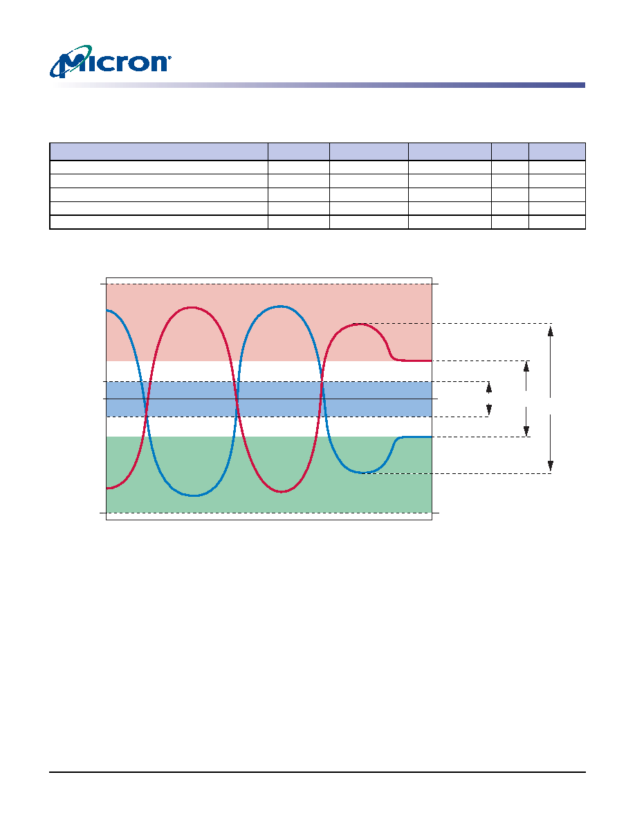
Figure 34:
SSTL_2 Clock Input
Notes: 1. This provides a minimum of 1.15V to a maximum of 1.35V, and is always half of VDDQ.
2. CK and CK# must cross in this region.
3. CK and CK# must meet at least VID(DC) MIN when static and is centered around VMP(DC)
4. CK and CK# must have a minimum 700mv peak to peak swing.
5. CK or CK# may not be more positive than VDDQ + 0.3V or more negative than Vss - 0.3V.
6. For AC operation, all DC clock requirements must also be satisfied.
7. Numbers in diagram reflect nominal values non-DDR400 devices.
Table 16:
Clock Input Operating Conditions
0°C
≤ T
A ≤ +70°C; VDDQ = +2.5V ±0.2V, VDD = +2.5V ±0.2V (VDDQ = +2.6V ±0.1V, VDD = +2.6V ±0.1V for DDR400)
Parameter/Condition
Symbol
Min
Max
Units
Notes
Clock input mid-point voltage; CK and CK#
VMP(DC)
1.15
1.35
V
Clock input voltage level; CK and CK#
VIN(DC)
-0.3
VDDQ + 0.3
Clock input differential voltage; CK and CK#
VID(DC)
0.36
VDDQ + 0.6
Clock input differential voltage; CK and CK#
VID(AC)
0.7
VDDQ + 0.6
Clock input crossing point voltage; CK and CK#
VIX(AC)
0.5 × VDDQ - 0.2 0.5 × VDDQ + 0.2
CK
CK#
2.80V
Maximum clock level
5
Minimum clock level
5
- 0.30V
1.25V
1.45V
1.05V
VID(AC)
4
VID(DC)
3
X
VMP(DC)
1
VIX(AC)
2
X
相關(guān)PDF資料 |
PDF描述 |
|---|---|
| MT46V128M4P-75ZLIT:C | 128M X 4 DDR DRAM, 0.75 ns, PDSO66 |
| MT46V64M4TG-75E | 64M X 4 DDR DRAM, 0.75 ns, PDSO66 |
| MT46V64M4FG-75Z | 64M X 4 DDR DRAM, 0.75 ns, PBGA60 |
| MT47H128M8HQ-3AT | 128M X 8 DDR DRAM, 0.4 ns, PBGA60 |
| MT47H64M16HR-3IT | 64M X 16 DDR DRAM, 0.4 ns, PBGA84 |
相關(guān)代理商/技術(shù)參數(shù) |
參數(shù)描述 |
|---|---|
| MT46V128M4T67A3WC1 | 制造商:Micron Technology Inc 功能描述:128MX4 DDR SDRAM DIE-COM COMMERCIAL 2.5V - Trays |
| MT46V128M4TG-5B/D | 制造商:Samsung Semiconductor 功能描述: |
發(fā)布緊急采購,3分鐘左右您將得到回復(fù)。