- 您現(xiàn)在的位置:買賣IC網(wǎng) > PDF目錄25631 > MPC8547VUATGA (FREESCALE SEMICONDUCTOR INC) 32-BIT, 1200 MHz, MICROPROCESSOR, CBGA783 PDF資料下載
參數(shù)資料
| 型號(hào): | MPC8547VUATGA |
| 廠商: | FREESCALE SEMICONDUCTOR INC |
| 元件分類: | 微控制器/微處理器 |
| 英文描述: | 32-BIT, 1200 MHz, MICROPROCESSOR, CBGA783 |
| 封裝: | 29 X 29 MM, 1 MM PITCH, FLIP CHIP, LEAD FREE, CERAMIC, BGA-783 |
| 文件頁(yè)數(shù): | 129/142頁(yè) |
| 文件大?。?/td> | 1504K |
| 代理商: | MPC8547VUATGA |
第1頁(yè)第2頁(yè)第3頁(yè)第4頁(yè)第5頁(yè)第6頁(yè)第7頁(yè)第8頁(yè)第9頁(yè)第10頁(yè)第11頁(yè)第12頁(yè)第13頁(yè)第14頁(yè)第15頁(yè)第16頁(yè)第17頁(yè)第18頁(yè)第19頁(yè)第20頁(yè)第21頁(yè)第22頁(yè)第23頁(yè)第24頁(yè)第25頁(yè)第26頁(yè)第27頁(yè)第28頁(yè)第29頁(yè)第30頁(yè)第31頁(yè)第32頁(yè)第33頁(yè)第34頁(yè)第35頁(yè)第36頁(yè)第37頁(yè)第38頁(yè)第39頁(yè)第40頁(yè)第41頁(yè)第42頁(yè)第43頁(yè)第44頁(yè)第45頁(yè)第46頁(yè)第47頁(yè)第48頁(yè)第49頁(yè)第50頁(yè)第51頁(yè)第52頁(yè)第53頁(yè)第54頁(yè)第55頁(yè)第56頁(yè)第57頁(yè)第58頁(yè)第59頁(yè)第60頁(yè)第61頁(yè)第62頁(yè)第63頁(yè)第64頁(yè)第65頁(yè)第66頁(yè)第67頁(yè)第68頁(yè)第69頁(yè)第70頁(yè)第71頁(yè)第72頁(yè)第73頁(yè)第74頁(yè)第75頁(yè)第76頁(yè)第77頁(yè)第78頁(yè)第79頁(yè)第80頁(yè)第81頁(yè)第82頁(yè)第83頁(yè)第84頁(yè)第85頁(yè)第86頁(yè)第87頁(yè)第88頁(yè)第89頁(yè)第90頁(yè)第91頁(yè)第92頁(yè)第93頁(yè)第94頁(yè)第95頁(yè)第96頁(yè)第97頁(yè)第98頁(yè)第99頁(yè)第100頁(yè)第101頁(yè)第102頁(yè)第103頁(yè)第104頁(yè)第105頁(yè)第106頁(yè)第107頁(yè)第108頁(yè)第109頁(yè)第110頁(yè)第111頁(yè)第112頁(yè)第113頁(yè)第114頁(yè)第115頁(yè)第116頁(yè)第117頁(yè)第118頁(yè)第119頁(yè)第120頁(yè)第121頁(yè)第122頁(yè)第123頁(yè)第124頁(yè)第125頁(yè)第126頁(yè)第127頁(yè)第128頁(yè)當(dāng)前第129頁(yè)第130頁(yè)第131頁(yè)第132頁(yè)第133頁(yè)第134頁(yè)第135頁(yè)第136頁(yè)第137頁(yè)第138頁(yè)第139頁(yè)第140頁(yè)第141頁(yè)第142頁(yè)
MPC8548E PowerQUICC III Integrated Processor Hardware Specifications, Rev. 5
Freescale Semiconductor
87
Package Description
18.2
Mechanical Dimensions of the HiCTE FC-CBGA and FC-PBGA
with Full Lid
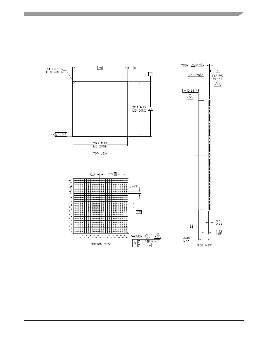
Figure 55 shows the mechanical dimensions and bottom surface nomenclature for both the MPC8548E
HiCTE FC-CBGA and FC-PBGA package with full lid.
Figure 55. Mechanical Dimensions and Bottom Surface Nomenclature of the HiCTE
FC-CBGA and FC-PBGA with Full Lid
Notes:
1. All d
imensions are in millimeters.
2. Dimensioning and tolerancing per ASME Y14.5M-1994.
3. Maximum solder ball diameter measured parallel to datum A.
4. Datum A, the seating plane, is determined by the spherical crowns of the solder balls.
5. Parallelism measurement shall exclude any effect of mark on top surface of package.
6. All dimensions are symmetric across the package center lines unless dimensioned otherwise.
7. Package code summary:
PBGA 8423
CBGA 5112
相關(guān)PDF資料 |
PDF描述 |
|---|---|
| MPC8548CHXATJ | 32-BIT, 1200 MHz, MICROPROCESSOR, CBGA783 |
| MPC8548ECHXAUGA | 32-BIT, 1333 MHz, MICROPROCESSOR, CBGA783 |
| MPC8548EHXAUHA | 32-BIT, 1333 MHz, MICROPROCESSOR, CBGA783 |
| MPC8548EVTAUGB | 32-BIT, 1333 MHz, MICROPROCESSOR, PBGA783 |
| MPC8548VTAVJB | 32-BIT, 1500 MHz, MICROPROCESSOR, PBGA783 |
相關(guān)代理商/技術(shù)參數(shù) |
參數(shù)描述 |
|---|---|
| MPC8547VUAUJ | 功能描述:微處理器 - MPU PQ38 8548 PB-FREE RoHS:否 制造商:Atmel 處理器系列:SAMA5D31 核心:ARM Cortex A5 數(shù)據(jù)總線寬度:32 bit 最大時(shí)鐘頻率:536 MHz 程序存儲(chǔ)器大小:32 KB 數(shù)據(jù) RAM 大小:128 KB 接口類型:CAN, Ethernet, LIN, SPI,TWI, UART, USB 工作電源電壓:1.8 V to 3.3 V 最大工作溫度:+ 85 C 安裝風(fēng)格:SMD/SMT 封裝 / 箱體:FBGA-324 |
| MPC8548CDS | 制造商:Freescale Semiconductor 功能描述:CDS DEV TOOLS FOR 8548 制造商:Freescale Semiconductor 功能描述:CDS DEV TOOLS FOR 8548 - Bulk 制造商:Freescale Semiconductor 功能描述:DEV TOOLS CDS FOR 8548 制造商:Freescale Semiconductor 功能描述:KIT MPC8548 CONFIG DEV SYSTEM |
| MPC8548CDS | 制造商:Freescale Semiconductor 功能描述:CDS DEV TOOLS FOR 8548 |
| MPC8548CHXAQG | 功能描述:微處理器 - MPU PQ38 8548 PB-FREE -40C RoHS:否 制造商:Atmel 處理器系列:SAMA5D31 核心:ARM Cortex A5 數(shù)據(jù)總線寬度:32 bit 最大時(shí)鐘頻率:536 MHz 程序存儲(chǔ)器大小:32 KB 數(shù)據(jù) RAM 大小:128 KB 接口類型:CAN, Ethernet, LIN, SPI,TWI, UART, USB 工作電源電壓:1.8 V to 3.3 V 最大工作溫度:+ 85 C 安裝風(fēng)格:SMD/SMT 封裝 / 箱體:FBGA-324 |
| MPC8548CPXAQGB | 功能描述:微處理器 - MPU FG PQ38 8548 RoHS:否 制造商:Atmel 處理器系列:SAMA5D31 核心:ARM Cortex A5 數(shù)據(jù)總線寬度:32 bit 最大時(shí)鐘頻率:536 MHz 程序存儲(chǔ)器大小:32 KB 數(shù)據(jù) RAM 大小:128 KB 接口類型:CAN, Ethernet, LIN, SPI,TWI, UART, USB 工作電源電壓:1.8 V to 3.3 V 最大工作溫度:+ 85 C 安裝風(fēng)格:SMD/SMT 封裝 / 箱體:FBGA-324 |
發(fā)布緊急采購(gòu),3分鐘左右您將得到回復(fù)。