- 您現(xiàn)在的位置:買賣IC網(wǎng) > PDF目錄245490 > VTC1-J55D-16M3676 (VECTRON INTERNATIONAL) TCVCXO, CLOCK, 16.3676 MHz, CMOS OUTPUT PDF資料下載
參數(shù)資料
| 型號: | VTC1-J55D-16M3676 |
| 廠商: | VECTRON INTERNATIONAL |
| 元件分類: | XO, clock |
| 英文描述: | TCVCXO, CLOCK, 16.3676 MHz, CMOS OUTPUT |
| 文件頁數(shù): | 5/8頁 |
| 文件大小: | 256K |
| 代理商: | VTC1-J55D-16M3676 |
VTC1 Data sheet
Vectron International 267 Lowell Rd, Hudson NH 03051
Tel: 1-88-VECTRON-1
e-mail: vectron@vectron.com
VCXO Functional Description
VCXO Feature: The VTC1 can be ordered with a VCXO function for applications were it will be used in a
PLL, or the output frequency needs fine tune adjustments. This is high impedance, 1 Mohm, input and can
be driven with an op-amp or terminated with adjustable resistors etc. Pin 1 should not be left floating on
the VCXO optional devices.
“No Adjust” Feature: In applications were the VTC1 will be not be used in a PLL, or the output frequency
does not fine tune adjustments, the best device to use would be a VTC1-x0xxx. By using the “no adjust”
option, the circuit is simplified as Vc does not need to adjusted or set to a predetermined voltage and pin 1
should be grounded or left open (but not set to a voltage such as the supply).
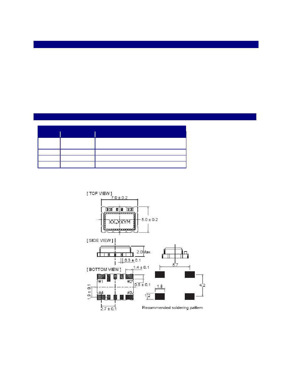
Outline Diagrams, Pad Layout and Pin Out
Table 3. Pinout
Pin #
Symbol
Function
1
N/C or
VC
No Connect (VTC1-x0xx)
or VCXO Control Voltage
2
GND
Electrical and Case Ground
3
fO
Output Frequency
4
VDD
Supply Voltage
NOTE: Additional pads are used to program and adjust the TCXO during manufacturing and should be left
open; do not terminate these to the supply voltage. Some designs do not include these additional pads.
Contact Pads are gold over nickel
Figure 3, Package drawing
相關(guān)PDF資料 |
PDF描述 |
|---|---|
| VTC1-J5BB-24M5535 | TCVCXO, CLOCK, 24.5535 MHz, CMOS OUTPUT |
| VTC1-J23A-24M8064 | TCVCXO, CLOCK, 24.8064 MHz, CMOS OUTPUT |
| VTC1-J43E-14M617188 | TCVCXO, CLOCK, 14.617188 MHz, CMOS OUTPUT |
| VTC1-J43E-16M368 | TCVCXO, CLOCK, 16.368 MHz, CMOS OUTPUT |
| VTC1-J55E-15M359865 | TCVCXO, CLOCK, 15.359865 MHz, CMOS OUTPUT |
相關(guān)代理商/技術(shù)參數(shù) |
參數(shù)描述 |
|---|---|
| VTC2 | 制造商:VECTRON 制造商全稱:Vectron International, Inc 功能描述:Voltage Controlled Temperature Compensated Crystal Oscillator |
| VTC21 | 制造商:VECTRON 制造商全稱:Vectron International, Inc 功能描述:Voltage Controlled Temperature Compensated Crystal Oscillator |
| VTC2H01A-10M000 | 制造商:VECTRON 制造商全稱:Vectron International, Inc 功能描述:Voltage Controlled Temperature Compensated Crystal Oscillator |
| VTC2H01B-10M000 | 制造商:VECTRON 制造商全稱:Vectron International, Inc 功能描述:Voltage Controlled Temperature Compensated Crystal Oscillator |
| VTC2H01C-10M000 | 制造商:VECTRON 制造商全稱:Vectron International, Inc 功能描述:Voltage Controlled Temperature Compensated Crystal Oscillator |
發(fā)布緊急采購,3分鐘左右您將得到回復(fù)。