- 您現(xiàn)在的位置:買賣IC網(wǎng) > PDF目錄29940 > TMM-140-04-F-D-SM-13-P-A (SAMTEC INC) 79 CONTACT(S), MALE, STRAIGHT TWO PART BOARD CONNECTOR, SURFACE MOUNT PDF資料下載
參數(shù)資料
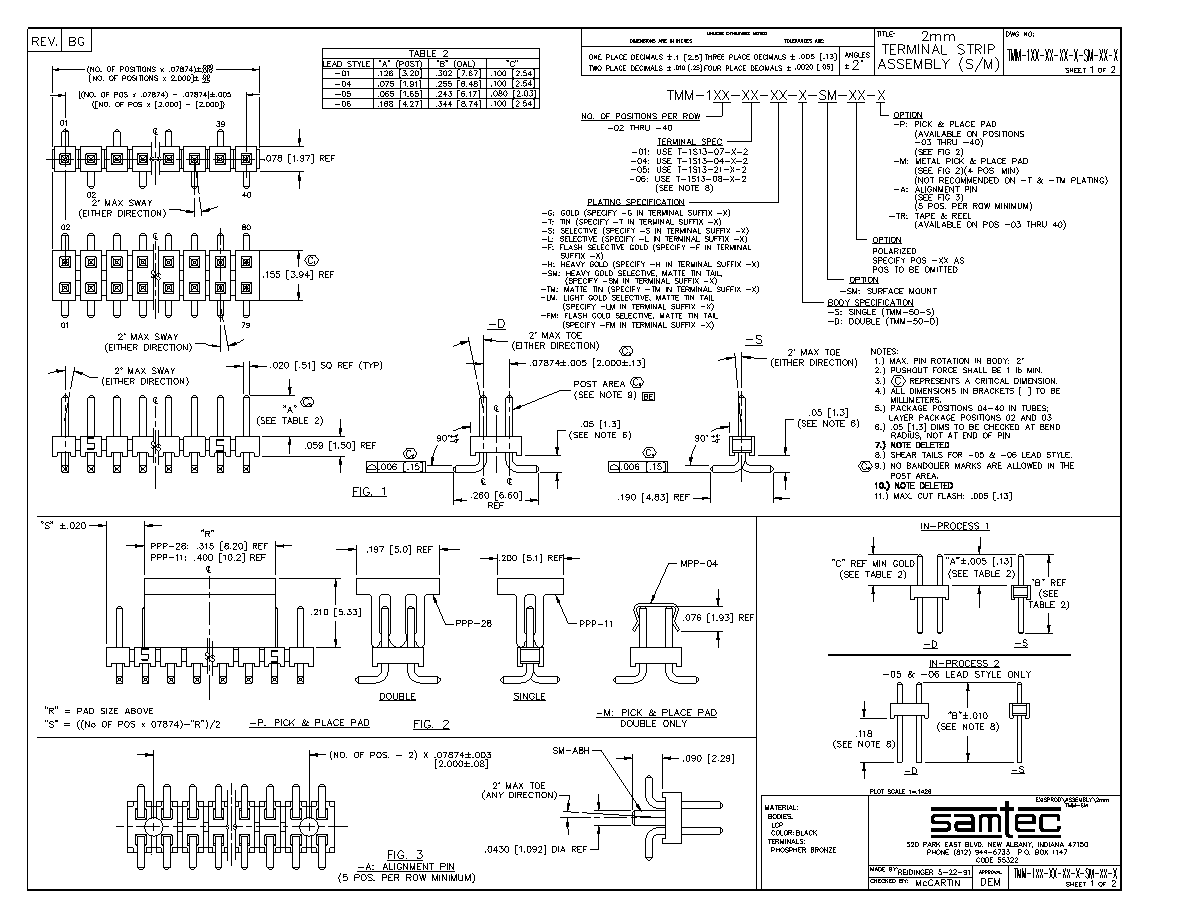
| 型號(hào): | TMM-140-04-F-D-SM-13-P-A |
| 廠商: | SAMTEC INC |
| 元件分類: | 電路板相疊連接器 |
| 英文描述: | 79 CONTACT(S), MALE, STRAIGHT TWO PART BOARD CONNECTOR, SURFACE MOUNT |
| 文件頁數(shù): | 1/1頁 |
| 文件大小: | 130K |
| 代理商: | TMM-140-04-F-D-SM-13-P-A |
相關(guān)PDF資料 |
PDF描述 |
|---|---|
| TMM-140-04-F-D-SM-14-P-TR | 79 CONTACT(S), MALE, STRAIGHT TWO PART BOARD CONNECTOR, SURFACE MOUNT |
| TMM-140-04-F-D-SM-16-P-M | 79 CONTACT(S), MALE, STRAIGHT TWO PART BOARD CONNECTOR, SURFACE MOUNT |
| TMM-140-04-F-D-SM-18-P-A | 79 CONTACT(S), MALE, STRAIGHT TWO PART BOARD CONNECTOR, SURFACE MOUNT |
| TMM-140-04-F-D-SM-25-P-M-A | 79 CONTACT(S), MALE, STRAIGHT TWO PART BOARD CONNECTOR, SURFACE MOUNT |
| TMM-140-04-F-D-SM-26-P-M-TR | 79 CONTACT(S), MALE, STRAIGHT TWO PART BOARD CONNECTOR, SURFACE MOUNT |
相關(guān)代理商/技術(shù)參數(shù) |
參數(shù)描述 |
|---|---|
| TMM-140-04-G-D | 制造商:Samtec Inc 功能描述:CONN UNSHRD HDR HDR 80 POS 2MM SLDR ST TH - Bulk |
| TMM-140-04-G-D-SM | 制造商:Samtec Inc 功能描述:CONN UNSHRD HDR HDR 80 POS 2MM SLDR ST SMD - Bulk |
| TMM-140-04-G-D-SM-A | 制造商:Samtec Inc 功能描述:CONN UNSHRD HDR HDR 80 POS 2MM SLDR ST SMD - Bulk |
| TMM-140-04-G-D-SM-A-M | 制造商:Samtec Inc 功能描述:CONN UNSHRD HDR HDR 80 POS 2MM SLDR ST SMD - Bulk |
| TMM-140-04-G-Q | 制造商:Samtec Inc 功能描述:CONN UNSHRD HDR HDR 160 POS 2MM SLDR ST TH - Bulk |
發(fā)布緊急采購,3分鐘左右您將得到回復(fù)。