- 您現(xiàn)在的位置:買賣IC網(wǎng) > PDF目錄358881 > LMH6732 (National Semiconductor Corporation) High Speed Op Amp with Adjustable Bandwidth PDF資料下載
參數(shù)資料
| 型號: | LMH6732 |
| 廠商: | National Semiconductor Corporation |
| 英文描述: | High Speed Op Amp with Adjustable Bandwidth |
| 中文描述: | 高速運算放大器帶寬可調(diào) |
| 文件頁數(shù): | 16/19頁 |
| 文件大小: | 970K |
| 代理商: | LMH6732 |
Application Information:
(Continued)
"POPLESS OUTPUT" & OFF CONDITION OUTPUT
STATE
The LMH6732 has been especially designed to have mini-
mum glitches during turn-on and turn-off. This is advanta-
geous in situations where the LMH6732 output is fed to
another stage which could experience false auto-ranging, or
even worse reset operation, due to these transient glitches.
Example of this application would be an AGC circuit or an
ADC with multiple ranges set to accommodate the largest
input amplitude. For the LMH6732, these sorts of transients
are typically less than 50mV in amplitude (see Electrical
Characteristics Tables for Typical values). Applications de-
signed to utilize the CLC505’s low output glitch would benefit
from using the LMH6732 instead since the LMH6732’s out-
put glitch is improved to be even lower than the CLC505’s. In
the "Off State", the output stage is turned off and is in effect
put into a high-Z state. In this sate, output can be forced by
other active devices. No significant current will flow through
the device output pin in this mode of operation.
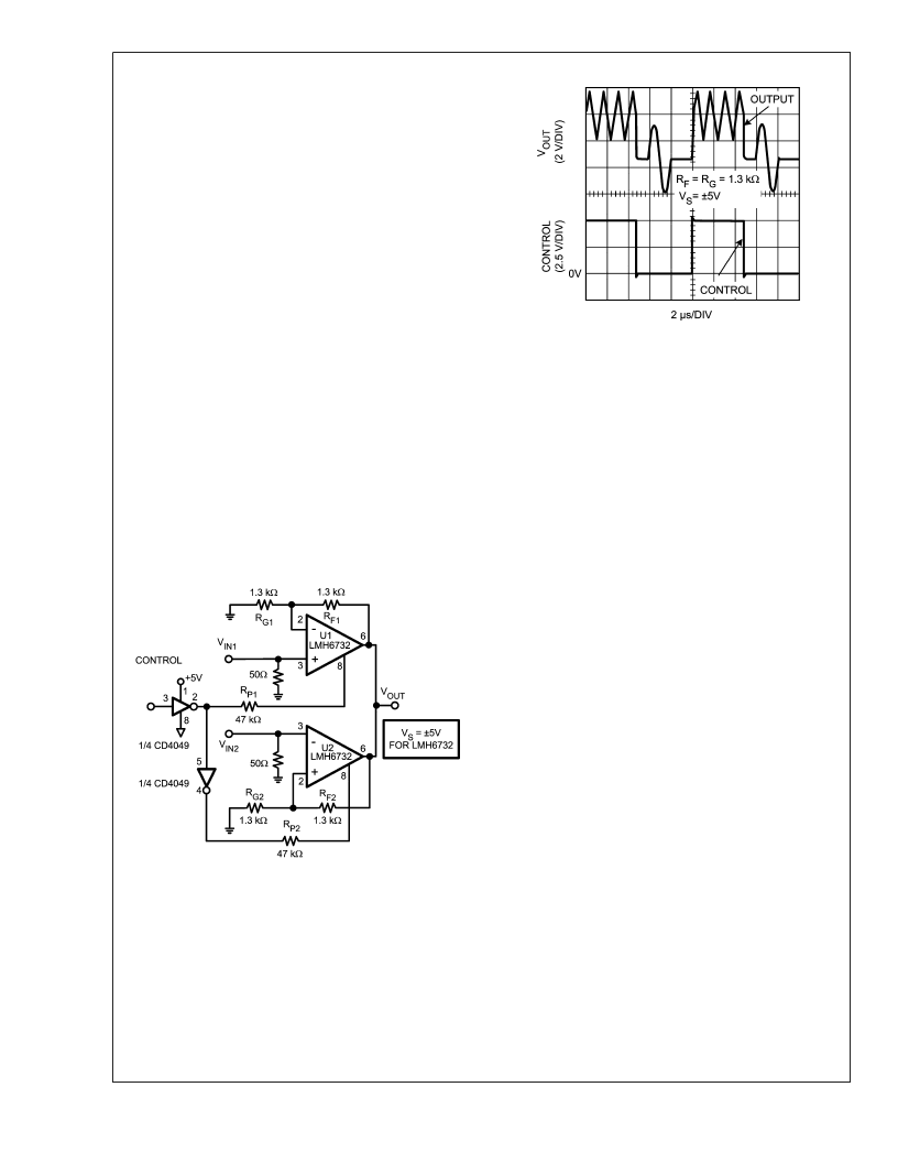
MUX APPLICATION
Since The LMH6732’s output is essentially open in the “off”
state, it is a good candidate for a fast 2:1 MUX.
Figure 6
shows one such application along with the output waveform
in
Figure 7
displaying the switching between a continuous
triangle wave and a single cycle sine wave (signals trigger
locked to each other for stable scope photo). Switching
speed of the MUX will be less than 50 ns and is governed by
the “Ton" and “Toff” times for U1 and U2 at the supply current
set by R
P1
and R
P2
. Note that the “Control” input is a 5V
CMOS logic level.
DIFFERENTIAL GAIN AND PHASE
Differential gain and phase are measurements useful prima-
rily in composite video channels. They are measured by
monitoring the gain and phase changes of a high frequency
carrier (3.58MHz for NTSC and 4.43MHz for PAL systems)
as the output of the amplifier is swept over a range of DC
voltages. Specifications for the LMH6732 include differential
gain and phase. Test signals used are based on a 1V
PP
video level. Test conditions used are the following:
DC sweep range: 0 to 100 IRE units (black to white)
Carrier: 4.43MHz at 40 IRE units peak to peak
A
V
= +2, R
L
= 75
+ 75
SOURCE IMPEDANCE
For best results, source impedance in the non-inverting cir-
cuit configuration (see
Figure 1
) should be kept below 5k
.
Above 5k
it is possible for oscillation to occur, depending
on other circuit board parasitics. For high signal source
impedances, a resistor with a value of less than 5k
may be
used to terminate the non-inverting input to ground.
FEEDBACK RESISTOR
In current-feedback op amps, the value of the feedback
resistor plays a major role in determining amplifier dynamics.
It is important to select the correct value. The LMH6732
provides optimum performance with feedback resistors as
shown in Table 2 below. Selection of an incorrect value can
lead to severe rolloff in frequency response, (if the resistor
value is too large) or , peaking or oscillation (if the value is
too low).
20060263
FIGURE 6. 50 ns 2:1 MUX Schematic
20060264
FIGURE 7. MUX “V
OUT
” and “Control” Waveform
L
www.national.com
16
相關(guān)PDF資料 |
PDF描述 |
|---|---|
| LMH6739 | Very Wideband, Low Distortion Triple Video Buffer |
| LMH6739MQ | Very Wideband, Low Distortion Triple Video Buffer |
| LMH6739MQX | Very Wideband, Low Distortion Triple Video Buffer |
| LMK316BJ475KL | UNREGULATED 60-mA CHARGE PUMP VOLTAGE INVERTER |
| LMK316BJ475ML | Low Drop Output Voltage Regulator |
相關(guān)代理商/技術(shù)參數(shù) |
參數(shù)描述 |
|---|---|
| LMH6732J | 制造商:Texas Instruments 功能描述: |
| LMH6732MA | 功能描述:運算放大器 - 運放 RoHS:否 制造商:STMicroelectronics 通道數(shù)量:4 共模抑制比(最小值):63 dB 輸入補(bǔ)償電壓:1 mV 輸入偏流(最大值):10 pA 工作電源電壓:2.7 V to 5.5 V 安裝風(fēng)格:SMD/SMT 封裝 / 箱體:QFN-16 轉(zhuǎn)換速度:0.89 V/us 關(guān)閉:No 輸出電流:55 mA 最大工作溫度:+ 125 C 封裝:Reel |
| LMH6732MA/NOPB | 功能描述:運算放大器 - 運放 Sgl 900Mhz Video Amp RoHS:否 制造商:STMicroelectronics 通道數(shù)量:4 共模抑制比(最小值):63 dB 輸入補(bǔ)償電壓:1 mV 輸入偏流(最大值):10 pA 工作電源電壓:2.7 V to 5.5 V 安裝風(fēng)格:SMD/SMT 封裝 / 箱體:QFN-16 轉(zhuǎn)換速度:0.89 V/us 關(guān)閉:No 輸出電流:55 mA 最大工作溫度:+ 125 C 封裝:Reel |
| LMH6732MAX | 功能描述:運算放大器 - 運放 RoHS:否 制造商:STMicroelectronics 通道數(shù)量:4 共模抑制比(最小值):63 dB 輸入補(bǔ)償電壓:1 mV 輸入偏流(最大值):10 pA 工作電源電壓:2.7 V to 5.5 V 安裝風(fēng)格:SMD/SMT 封裝 / 箱體:QFN-16 轉(zhuǎn)換速度:0.89 V/us 關(guān)閉:No 輸出電流:55 mA 最大工作溫度:+ 125 C 封裝:Reel |
| LMH6732MAX/NOPB | 功能描述:運算放大器 - 運放 RoHS:否 制造商:STMicroelectronics 通道數(shù)量:4 共模抑制比(最小值):63 dB 輸入補(bǔ)償電壓:1 mV 輸入偏流(最大值):10 pA 工作電源電壓:2.7 V to 5.5 V 安裝風(fēng)格:SMD/SMT 封裝 / 箱體:QFN-16 轉(zhuǎn)換速度:0.89 V/us 關(guān)閉:No 輸出電流:55 mA 最大工作溫度:+ 125 C 封裝:Reel |
發(fā)布緊急采購,3分鐘左右您將得到回復(fù)。