- 您現(xiàn)在的位置:買賣IC網(wǎng) > PDF目錄4179 > EP2SGX130GF40C4ES (Altera)IC STRATIX II GX 130K 1508-FBGA PDF資料下載
參數(shù)資料
| 型號: | EP2SGX130GF40C4ES |
| 廠商: | Altera |
| 文件頁數(shù): | 203/1486頁 |
| 文件大小: | 0K |
| 描述: | IC STRATIX II GX 130K 1508-FBGA |
| 標(biāo)準(zhǔn)包裝: | 3 |
| 系列: | Stratix® II GX |
| LAB/CLB數(shù): | 6627 |
| 邏輯元件/單元數(shù): | 132540 |
| RAM 位總計: | 6747840 |
| 輸入/輸出數(shù): | 734 |
| 電源電壓: | 1.15 V ~ 1.25 V |
| 安裝類型: | 表面貼裝 |
| 工作溫度: | 0°C ~ 70°C |
| 封裝/外殼: | 1508-BBGA |
| 供應(yīng)商設(shè)備封裝: | 1508-FBGA(30x30) |
| 其它名稱: | 544-1743 |
9–34
Altera Corporation
Stratix II GX Device Handbook, Volume 2
October 2007
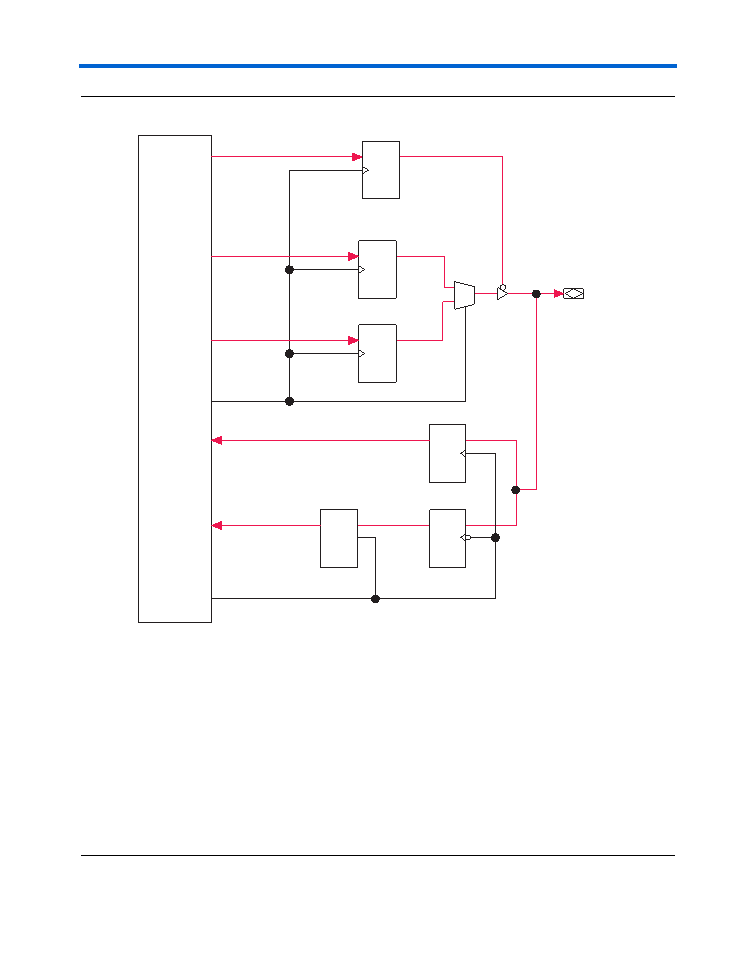
Stratix II and Stratix II GX DDR Memory Support Overview
Figure 9–15. DQ Configuration in Stratix II or Stratix II GX IOE
Notes to Figure 9–15:
(1)
You can use the altdq megafunction to generate the DQ signals. You should, however, use Altera’s memory
controller IP Tool Bench to generate the data path for your memory interface. The signal names used here match
with Quartus II software naming convention.
(2)
The OE signal is active low, but the Quartus II software implements this as active high and automatically adds an
inverter before the OE register AOE during compilation.
(3)
The outclock signal for DDR, DDR2 SDRAM, and QDRII SRAM interfaces has a 90° phase-shift relationship with
the system clock. For 300-MHz RLDRAM II interfaces with EP2S60F1020C3, Altera recommends a 75° phase-shift
relationship.
(4)
The shifted DQS or DQSn signal can clock this register. Only use the DQSn signal for QDRII SRAM interfaces.
(5)
The shifted DQS signal must be inverted before going to the DQ IOE. The inversion is automatic if you use the
altdq
megafunction to generate the DQ signals. Connect this port to the combout port in the altdqs
megafunction.
(6)
On the top and bottom I/O banks, the clock to this register can be an inverted register A’s clock or a separate clock
(inverted or non-inverted). On the side I/O banks, you can only use the inverted register A’s clock for this port.
D
Q
DFF
D
Q
LA
TCH
ENA
D
Q
DFF
Input Register AI
Input Register BI
Latch C
DQ
DFF
DQ
DFF
0
1
DQ
DFF
TRI
DQ Pin
OE Register AOE
Output Register AO
Output Register BO
Logic Array
Latch
dataout_l
dataout_h
outclock (3)
datain_h
datain_l
OE
inclock (from DQS bus)
neg_reg_out
I
(5)
(4)
(2)
(6)
相關(guān)PDF資料 |
PDF描述 |
|---|---|
| EP2SGX130GF40C3N | IC STRATIX II GX 130K 1508-FBGA |
| EP2SGX130GF1508C3 | IC STRATIX II GX 130K 1508-FBGA |
| EP20K100FC324-1V | IC APEX 20K FPGA 100K 208-PQFP |
| A1425A-PLG84I | IC FPGA 2500 GATES 84-PLCC |
| ACB106DHHT-S578 | EDGECARD 212POS .050 SLD W/POSTS |
相關(guān)代理商/技術(shù)參數(shù) |
參數(shù)描述 |
|---|---|
| EP2SGX130GF40C4NES | 功能描述:IC STRATIX II GX 130K 1508-FBGA RoHS:是 類別:集成電路 (IC) >> 嵌入式 - FPGA(現(xiàn)場可編程門陣列) 系列:Stratix® II GX 產(chǎn)品變化通告:XC4000(E,L) Discontinuation 01/April/2002 標(biāo)準(zhǔn)包裝:24 系列:XC4000E/X LAB/CLB數(shù):100 邏輯元件/單元數(shù):238 RAM 位總計:3200 輸入/輸出數(shù):80 門數(shù):3000 電源電壓:4.5 V ~ 5.5 V 安裝類型:表面貼裝 工作溫度:-40°C ~ 100°C 封裝/外殼:120-BCBGA 供應(yīng)商設(shè)備封裝:120-CPGA(34.55x34.55) |
| EP2SGX130GF40C5 | 功能描述:IC STRATIX II GX 130K 1508-FBGA RoHS:否 類別:集成電路 (IC) >> 嵌入式 - FPGA(現(xiàn)場可編程門陣列) 系列:Stratix® II GX 產(chǎn)品變化通告:XC4000(E,L) Discontinuation 01/April/2002 標(biāo)準(zhǔn)包裝:24 系列:XC4000E/X LAB/CLB數(shù):100 邏輯元件/單元數(shù):238 RAM 位總計:3200 輸入/輸出數(shù):80 門數(shù):3000 電源電壓:4.5 V ~ 5.5 V 安裝類型:表面貼裝 工作溫度:-40°C ~ 100°C 封裝/外殼:120-BCBGA 供應(yīng)商設(shè)備封裝:120-CPGA(34.55x34.55) |
| EP2SGX130GF40C5NES | 功能描述:IC STRATIX II GX 130K 1508-FBGA RoHS:是 類別:集成電路 (IC) >> 嵌入式 - FPGA(現(xiàn)場可編程門陣列) 系列:Stratix® II GX 產(chǎn)品變化通告:XC4000(E,L) Discontinuation 01/April/2002 標(biāo)準(zhǔn)包裝:24 系列:XC4000E/X LAB/CLB數(shù):100 邏輯元件/單元數(shù):238 RAM 位總計:3200 輸入/輸出數(shù):80 門數(shù):3000 電源電壓:4.5 V ~ 5.5 V 安裝類型:表面貼裝 工作溫度:-40°C ~ 100°C 封裝/外殼:120-BCBGA 供應(yīng)商設(shè)備封裝:120-CPGA(34.55x34.55) |
| EP2SGX30 | 制造商:ALTERA 制造商全稱:Altera Corporation 功能描述:Package Information Datasheet for Mature Altera Devices |
| EP2SGX30C | 制造商:ALTERA 制造商全稱:Altera Corporation 功能描述:Stratix II GX Device |
發(fā)布緊急采購,3分鐘左右您將得到回復(fù)。