- 您現在的位置:買賣IC網 > PDF目錄211783 > CLC432AJE-TR13 (NATIONAL SEMICONDUCTOR CORP) DUAL OP-AMP, 7000 uV OFFSET-MAX, 92 MHz BAND WIDTH, PDSO8 PDF資料下載
參數資料
| 型號: | CLC432AJE-TR13 |
| 廠商: | NATIONAL SEMICONDUCTOR CORP |
| 元件分類: | 運算放大器 |
| 英文描述: | DUAL OP-AMP, 7000 uV OFFSET-MAX, 92 MHz BAND WIDTH, PDSO8 |
| 封裝: | PLASTIC, SOIC-8 |
| 文件頁數: | 2/27頁 |
| 文件大小: | 685K |
| 代理商: | CLC432AJE-TR13 |
第1頁當前第2頁第3頁第4頁第5頁第6頁第7頁第8頁第9頁第10頁第11頁第12頁第13頁第14頁第15頁第16頁第17頁第18頁第19頁第20頁第21頁第22頁第23頁第24頁第25頁第26頁第27頁
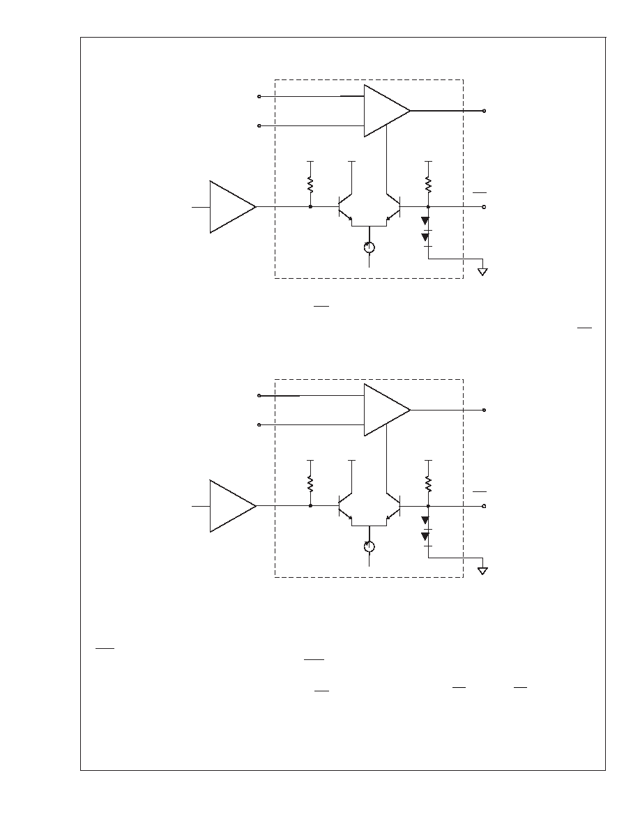
Application Division (Continued)
The disable feature of the CLC431 is such that DIS and DIS
have common-mode input voltage ranges of (+V
CC)to
(V
CC+3V) and are so guaranteed over the commercial
temperature range. Internal clamps (not shown) protect the
DIS input from excessive input voltages that could otherwise
cause damage to the device. This condition occurs when
enough source current flows into the node so as to allow DIS
to rise to V
CC. This clamp is activated once DIS exceeds DIS
by 1.5Volts and guarantees that V
DIS(ground referenced)
does not exceed 4.7Volts.
Figure 2 illustrates the differential mode of the CLC431’s
disable feature for ECL-type logic. In order for this mode to
operate properly, V
RTTL must be left floating while DIS and
DIS are to be connected directly to the ECL gate as illus-
trated. Applying a differential logic “high” (DIS - DIS
≥
0.4Volts) switches the tail current of the differential pair from
Q2 to Q1 and results in the disabling of that CLC431 chan-
nel. Alternatively, applying a differential logic “l(fā)ow” (DIS - DIS
≤ 0.4Volts) switches the tail current of the differential pair
from Q1 to Q2 and results in the enabling of that same
channel. The internal clamp, mentioned above, also protects
against excessive differential voltages up to 30 Volts while
limiting input currents to <3mA.
DC Performance
A current-feedback amplifier’s input stage does not have
equal nor correlated bias currents, therefore they cannot be
cancelled and each contributes to the total DC offset voltage
at the output by the following equation:
VI
R
V
R
IR
offset
bn
s
f
g
io
f
g
bi
f
=±
+
++
+
11
(1)
The input resistor R
s is that resistance seen when looking
from the non-inverting input back towards the source. For
inverting DC-offset calculations, the source resistance seen
VRTTL
+VCC
DIS
Vnon-inv
Vinv
Vout
CLC431
100k
100k
Q1
Q2
TTL
CMOS
+
-
DS012712-27
FIGURE 1.
VRTTL
+VCC
DIS
Vnon-inv
Vinv
Vout
CLC431
100k
100k
Q1
Q2
TTL
CMOS
+
-
DS012712-27
FIGURE 2.
CLC431/432
www.national.com
10
相關PDF資料 |
PDF描述 |
|---|---|
| CD6338C | 39 V, SILICON, UNIDIRECTIONAL VOLTAGE REGULATOR DIODE |
| CD6338D | 39 V, SILICON, UNIDIRECTIONAL VOLTAGE REGULATOR DIODE |
| CD6339C | 43 V, SILICON, UNIDIRECTIONAL VOLTAGE REGULATOR DIODE |
| CD6339 | 43 V, SILICON, UNIDIRECTIONAL VOLTAGE REGULATOR DIODE |
| CD6344C | 68 V, SILICON, UNIDIRECTIONAL VOLTAGE REGULATOR DIODE |
相關代理商/技術參數 |
參數描述 |
|---|---|
| CLC432AJP | 制造商:Rochester Electronics LLC 功能描述:- Bulk |
| CLC432AJ-QML | 制造商:未知廠家 制造商全稱:未知廠家 功能描述:Current-Feedback Operational Amplifier |
| CLC436 | 制造商:NSC 制造商全稱:National Semiconductor 功能描述:200MHz, 【15V, Low-Power Voltage Feedback Op Amp |
| CLC436AJ | 制造商:NSC 制造商全稱:National Semiconductor 功能描述:200MHz, 【15V, Low-Power Voltage Feedback Op Amp |
| CLC436AJP | 制造商:NSC 制造商全稱:National Semiconductor 功能描述:IC-FEEDBACK OP-AMP |
發(fā)布緊急采購,3分鐘左右您將得到回復。