- 您現(xiàn)在的位置:買賣IC網(wǎng) > PDF目錄166731 > BU-65142D1-480K Controller Miscellaneous - Datasheet Reference PDF資料下載
參數(shù)資料
| 型號(hào): | BU-65142D1-480K |
| 英文描述: | Controller Miscellaneous - Datasheet Reference |
| 中文描述: | 控制器雜項(xiàng)-數(shù)據(jù)表參考 |
| 文件頁數(shù): | 20/24頁 |
| 文件大小: | 219K |
| 代理商: | BU-65142D1-480K |
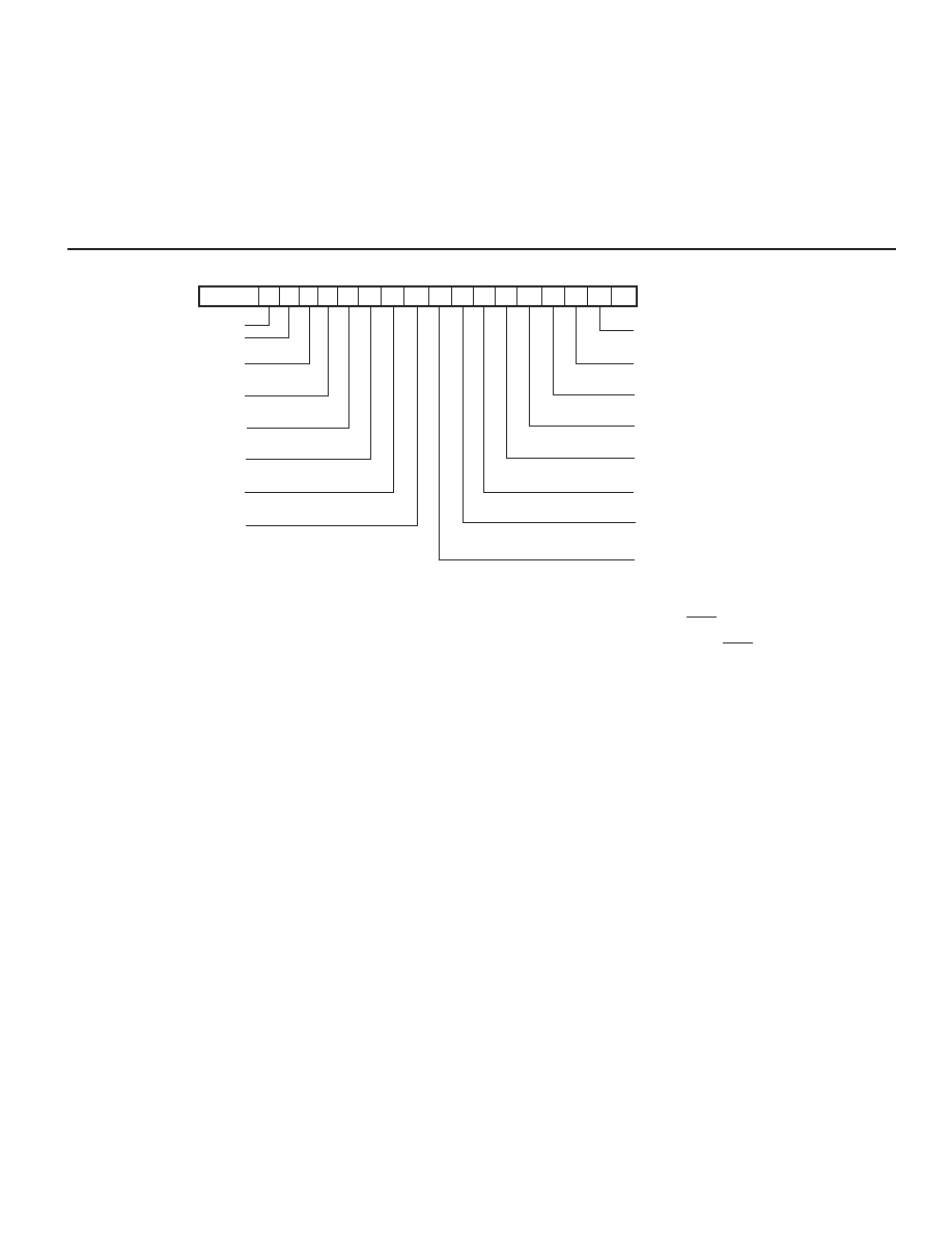
BUILT-IN-TEST
The BUS-65142 contains a 14-bit Built-In-Test (BIT) word regis-
ter which stores information about the condition of the RTU.
When a mode code is received to transmit the BIT word, the con-
tents of the BIT register is transmitted over the 1553 bus.
FIGURE 2 shows the fault assigned to each bit in the BIT word.
Conditions monitored are; transmitter timeouts, loop test failures,
transmitter shutdown, subsystem handshake failure, and the
results of individual message validations.
5
FIGURE 2. BUILT-IN-TEST (BIT) WORD REGISTER
DATA SYNC
15
14
13
12
11
10
9
8
7
6
5
4
3
2
1
0
P
CHANNEL A/B - TRANSMITTER TIMEOUT
HANDSHAKE FAILURE
CHANNEL A/B - LOOP TEST FAILURE
MODE CODE - T/R ERROR
{
ILLEGAL OR RESERVED MODE CODE
ILLEGAL USE OF BROADCAST WITH MODE CODE
MESSAGE SERVICING ABORTED DUE TO LOW WORD COUNT
MESSAGE SERVICING ABORTED DUE TO HIGH WORD COUNT
NON-MODE BROADCAST COMMAND TO TRANSMIT
ALWAYS ZERO
CHANNEL B - TRANSMITTER TIMEOUT
CHANNEL B - LOOP TEST FAILURE
CHANNEL B - TRANSMITTER SHUTDOWN
CHANNEL A - LOOP TEST FAILURE
CHANNEL A - TRANSMITTER SHUTDOWN
CHANNEL A TRANSMITTER TIMEOUT
1. BITS 3-7 ARE CLEARED IN THE BEGINNING OF EACH NEW MESSAGE AND UPDATED AT THE END OF THE MESSAGE.
THEY ONLY REFLECT THE PRESENT COMMAND WORD.
2. BITS 0-2 AND 10-13 ARE LATCHED AND ONLY CLEARED BY A MODE RESET COMMAND OR A MASTER RESET (RESET).
NOTES
3. BITS 8 AND 9 ARE SET ONLY BY THE MODE COMMAND FOR "TRANSMITTER SHUTDOWN" AND ARE CLEARED BY THE MODE COMMAND
FOR "OVERRIDE TRANSMITTER SHUTDOWN" OR "RESET REMOTE TERMINAL". BITS 8 AND 9 ARE ALSO CLEARED BY RESET.
{
相關(guān)PDF資料 |
PDF描述 |
|---|---|
| BU-65142D1-480L | CABLE BULK (3) THIN LINE 250' |
| BU-65142D1-480Q | Controller Miscellaneous - Datasheet Reference |
| BU-65142D1-480S | CA KVM HD15/(2)MD6 M-F 10' |
| BU-65142D1-480W | CA KVM HD15/(2)MD6 M-F 20' |
| BU-65142D1-480Y | CA KVM HD15/(2)MD6 M-F 3' |
相關(guān)代理商/技術(shù)參數(shù) |
參數(shù)描述 |
|---|---|
| BU65170G0-100 | 制造商:未知廠家 制造商全稱:未知廠家 功能描述:Interface IC |
| BU65170G0-110 | 制造商:未知廠家 制造商全稱:未知廠家 功能描述:Interface IC |
| BU65170G0-120 | 制造商:未知廠家 制造商全稱:未知廠家 功能描述:Interface IC |
| BU65170G0-200 | 制造商:未知廠家 制造商全稱:未知廠家 功能描述:Interface IC |
| BU65170G0-300 | 制造商:未知廠家 制造商全稱:未知廠家 功能描述:Interface IC |
發(fā)布緊急采購,3分鐘左右您將得到回復(fù)。