- 您現(xiàn)在的位置:買賣IC網(wǎng) > PDF目錄384007 > TLE4945 (INFINEON TECHNOLOGIES AG) Uni- and Bipolar Hall IC Switches for Magnetic Field Applications PDF資料下載
參數(shù)資料
| 型號: | TLE4945 |
| 廠商: | INFINEON TECHNOLOGIES AG |
| 英文描述: | Uni- and Bipolar Hall IC Switches for Magnetic Field Applications |
| 中文描述: | 單極和雙極霍爾集成電路開關磁場應用 |
| 文件頁數(shù): | 6/13頁 |
| 文件大小: | 84K |
| 代理商: | TLE4945 |
TLE 4905 G; TLE 4935 G
TLE 4935-2 G; TLE 4945-2 G
Data Sheet
6
2000-07-01
Note: Stresses above those listed here may cause permanent damage to the device.
Exposure to absolute maximum rating conditions for extended periods may affect
device reliability.
Note: In the operating range the functions given in the circuit description are fulfilled.
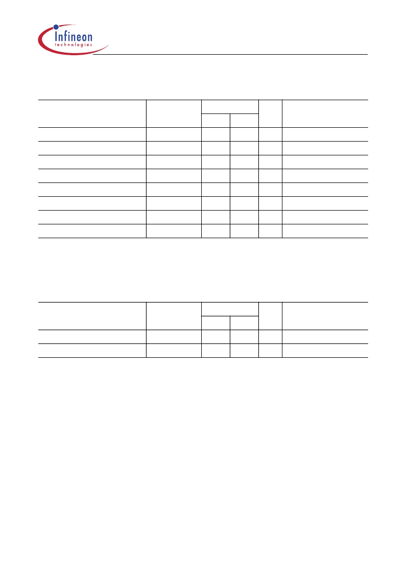
Absolute Maximum Ratings
T
j
= – 40 to 150
°
C
Parameter
Symbol
Limit Values Unit Remarks
min.
max.
– 40
32
V
–
40
V
–
32
V
–
100
mA
–
100
mA
– 40
150
°
C
– 50
150
°
C
100
K/W –
Supply voltage
Supply voltage
Output voltage
Output current
Output reverse current
Junction temperature
Storage temperature
Thermal resistance
V
S
V
S
V
Q
I
Q
–
I
Q
T
j
T
stg
R
th JA
–
t
ν
= 0.1
–
–
–
–
–
Operating Range
Parameter
Symbol
Limit Values Unit Remarks
min.
max.
4.0
24
V
– 40
150
°
C
Supply voltage
Junction temperature
V
S
T
j
–
–
相關PDF資料 |
PDF描述 |
|---|---|
| TLE4945L | Uni- and Bipolar Hall IC Switches for Magnetic Field Applications |
| TLE4905G | Unipolar Hall IC Switches for Magnetic Field Applications(用于磁場應用的單極霍爾芯片開關) |
| TLE4935G | Bipolar Hall IC Switches for Magnetic Field Applications(用于磁場應用的雙極霍爾芯片開關) |
| TLE4935-2G | Bipolar Hall IC Switches for Magnetic Field Applications(用于磁場應用的雙極霍爾芯片開關) |
| TLE4946H | High Precision Hall-Effect Switch |
相關代理商/技術參數(shù) |
參數(shù)描述 |
|---|---|
| TLE4945-2G | 功能描述:板機接口霍耳效應/磁性傳感器 Bipolar 4V - 24V 5 mA RoHS:否 制造商:Honeywell 類型:Bipolar Hall-Effect Digital Position Sensor 工作電源電壓:3 V to 24 V 電源電流:3.5 mA 最大輸出電流:20 mA 工作點最小值/最大值:5 G, 55 G 最小/最大釋放點(Brp):- 55 G, - 5 G 最大工作溫度:+ 150 C 安裝風格:SMD/SMT 封裝 / 箱體:SOT-23 |
| TLE49452GNT | 制造商:Infineon Technologies AG 功能描述:Hall Effect Sensor 100mA Bipolar 5V/9V/12V/15V/18V 4-Pin(3+Tab) SOT-89 T/R |
| TLE4945-2L | 功能描述:板機接口霍耳效應/磁性傳感器 UNI/BIPOLAR HALL IC SWITCH FOR MAG FIELD RoHS:否 制造商:Honeywell 類型:Bipolar Hall-Effect Digital Position Sensor 工作電源電壓:3 V to 24 V 電源電流:3.5 mA 最大輸出電流:20 mA 工作點最小值/最大值:5 G, 55 G 最小/最大釋放點(Brp):- 55 G, - 5 G 最大工作溫度:+ 150 C 安裝風格:SMD/SMT 封裝 / 箱體:SOT-23 |
| TLE49452LHALA1 | 制造商:Infineon Technologies AG 功能描述:Hall Effect Sensor 100mA Bipolar 5V/9V/12V/15V/18V T/R 制造商:Infineon Technologies AG 功能描述:MAGNETIC SENSOR IC'S - Ammo Pack |
| TLE4945L | 功能描述:板機接口霍耳效應/磁性傳感器 Bipolar 3.8V - 24V 8 mA RoHS:否 制造商:Honeywell 類型:Bipolar Hall-Effect Digital Position Sensor 工作電源電壓:3 V to 24 V 電源電流:3.5 mA 最大輸出電流:20 mA 工作點最小值/最大值:5 G, 55 G 最小/最大釋放點(Brp):- 55 G, - 5 G 最大工作溫度:+ 150 C 安裝風格:SMD/SMT 封裝 / 箱體:SOT-23 |
發(fā)布緊急采購,3分鐘左右您將得到回復。