- 您現(xiàn)在的位置:買賣IC網(wǎng) > PDF目錄163690 > 95611-203H 3 CONTACT(S), MALE, STRAIGHT BOARD STACKING CONNECTOR, SOLDER PDF資料下載
參數(shù)資料
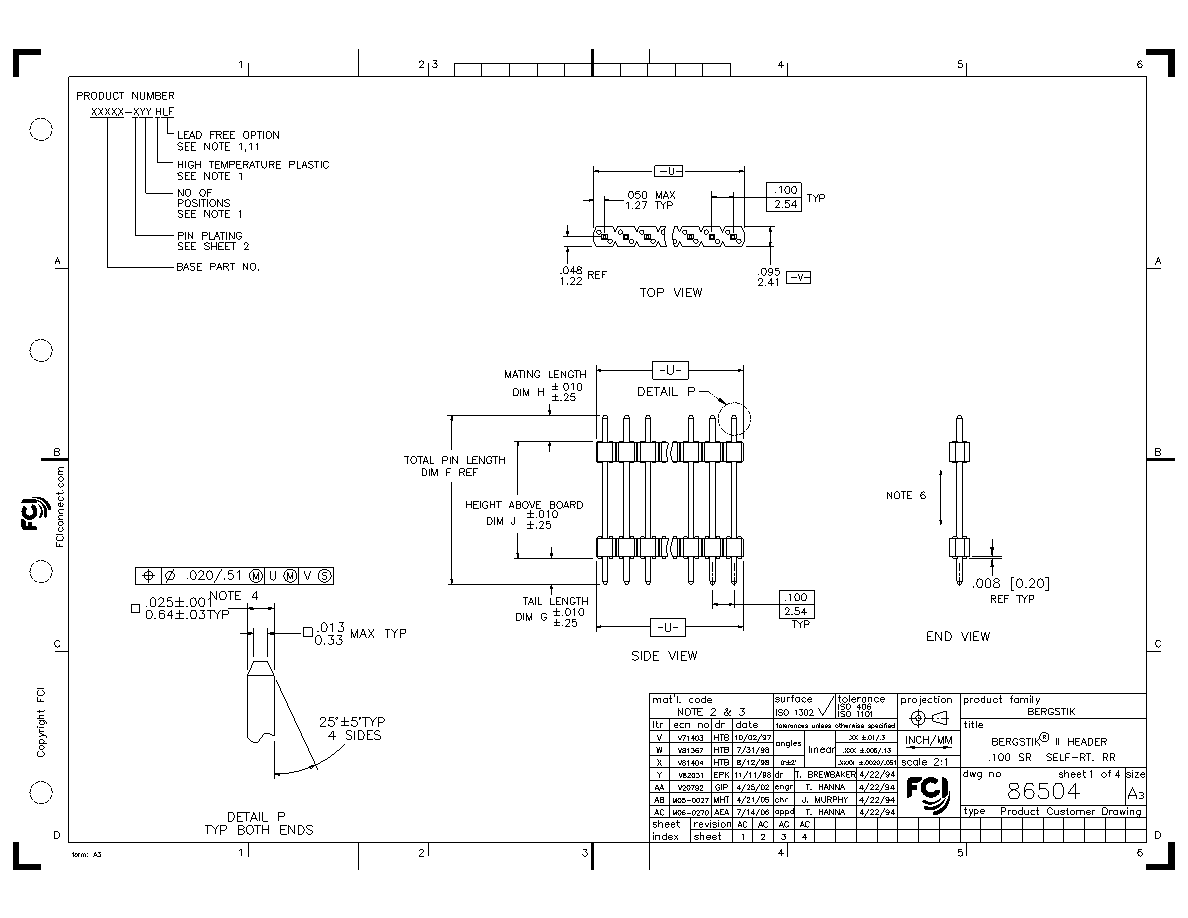
| 型號: | 95611-203H |
| 元件分類: | 電路板相疊連接器 |
| 英文描述: | 3 CONTACT(S), MALE, STRAIGHT BOARD STACKING CONNECTOR, SOLDER |
| 文件頁數(shù): | 1/4頁 |
| 文件大小: | 297K |
| 代理商: | 95611-203H |
PDM: Rev:AC
Released
.
STATUS:
Printed: Jul 20, 2006
相關(guān)PDF資料 |
PDF描述 |
|---|---|
| 95611-204H | 4 CONTACT(S), MALE, STRAIGHT BOARD STACKING CONNECTOR, SOLDER |
| 95611-205HLF | 5 CONTACT(S), MALE, STRAIGHT BOARD STACKING CONNECTOR, SOLDER |
| 95611-206HLF | 6 CONTACT(S), MALE, STRAIGHT BOARD STACKING CONNECTOR, SOLDER |
| 95611-206H | 6 CONTACT(S), MALE, STRAIGHT BOARD STACKING CONNECTOR, SOLDER |
| 95611-207HLF | 7 CONTACT(S), MALE, STRAIGHT BOARD STACKING CONNECTOR, SOLDER |
相關(guān)代理商/技術(shù)參數(shù) |
參數(shù)描述 |
|---|---|
| 956-120-5000 | 制造商:Amphenol Corporation 功能描述:LC ADAPTER, SIMPLEX - Bulk |
| 956-120-5200 | 制造商:Amphenol Corporation 功能描述:LC ADAPTER, DUPLEX - Bulk |
| 956-130-5108 | 制造商:Amphenol Corporation 功能描述: |
| 956135-2B | 制造商:VISH 功能描述: 制造商:Vishay Intertechnologies 功能描述: |
| 95614-BX | 功能描述:ACCESSORY 制造商:littelfuse inc. 系列:* 零件狀態(tài):停產(chǎn) 標(biāo)準(zhǔn)包裝:1 |
發(fā)布緊急采購,3分鐘左右您將得到回復(fù)。