- 您現(xiàn)在的位置:買賣IC網(wǎng) > PDF目錄202872 > VTC1-A23B-14M5888 (VECTRON INTERNATIONAL) TCVCXO, CLIPPED SINE OUTPUT, 14.5888 MHz PDF資料下載
參數(shù)資料
| 型號(hào): | VTC1-A23B-14M5888 |
| 廠商: | VECTRON INTERNATIONAL |
| 元件分類: | TCVCXO, sine |
| 英文描述: | TCVCXO, CLIPPED SINE OUTPUT, 14.5888 MHz |
| 文件頁數(shù): | 3/8頁 |
| 文件大?。?/td> | 256K |
| 代理商: | VTC1-A23B-14M5888 |
VTC1 Data sheet
Vectron International 267 Lowell Rd, Hudson NH 03051
Tel: 1-88-VECTRON-1
e-mail: vectron@vectron.com
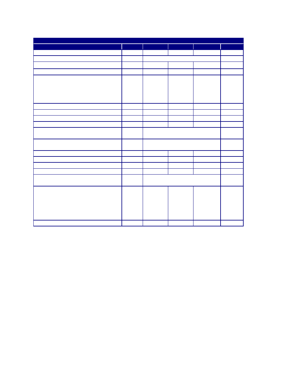
Table 2. Electrical Performance for the CMOS Output Option
Parameter
Symbol
Min
Typical
Maximum
Units
Frequency
fO
10.000
40.000
MHz
Supply Voltage
3.3V±10%
VDC
Maximum Supply Voltage
7
VDC
Supply Current
IDD
10.0
mA
Output Level
2
Logic High
Logic Low
Drive High
Drive Low
VOH
VOL
IOH
IOL
0.9*VDD
4
0.1*VDD
-4
V
mA
Output Load
15pf
Duty Cycle, @ 50%
45/55
%
Control Voltage Impedance
ZVc
100
Kohm
Control Voltage to reach pull
0.5
2.5
V
Pull Range
Ordering option, see last page
TPR
±5, ±8, ±10
ppm
Temperature Stability
Ordering option, see last page.
±0.5 to ±5.0
ppm
Initial Accuracy, “No Adjust” option
±0.5
ppm
Power Supply Stability
±0.3
ppm
Load Stability
±0.2
ppm
Aging
±1.0
ppm/year
Operating temperature
Ordering option, see last page
0/55, -10/60, -20/70, -30/80, -40/85
°C
Phase Noise, 12.800MHz
10 Hz offset
100 Hz offset
1 kHz offset
10 kHz offset
100 kHz offset
-93
-123
-147
-155
-158
dBc/Hz
Start-up time
2
ms
1. A 0.01uF and a 0.1uF capacitor should be located as close to the supply as possible (to ground) is recommended.
2. Output is DC coupled.
相關(guān)PDF資料 |
PDF描述 |
|---|---|
| VTC1-A23C-14M5888 | TCVCXO, CLIPPED SINE OUTPUT, 14.5888 MHz |
| VTC1-A23C-16M384 | TCVCXO, CLIPPED SINE OUTPUT, 16.384 MHz |
| VTC1-B31B-16M034950 | TCVCXO, CLIPPED SINE OUTPUT, 16.03495 MHz |
| VTC1-B2BB-26M000 | TCVCXO, CLIPPED SINE OUTPUT, 26 MHz |
| VTC1-B2BC-16M368 | TCVCXO, CLIPPED SINE OUTPUT, 16.368 MHz |
相關(guān)代理商/技術(shù)參數(shù) |
參數(shù)描述 |
|---|---|
| VTC1-B01E-10M000000 | 功能描述:TCVCXO振蕩器 10MHz 3.3Volts 1.0ppm -40C +85C RoHS:否 制造商:Pletronics Inc. 封裝 / 箱體:LCC 頻率:10 MHz 頻率穩(wěn)定性:50 PPB 負(fù)載電容: 端接類型:SMD/SMT 尺寸:3.2 mm W x 5 mm L x 1.5 mm H 電源電壓:3.3 V 最小工作溫度:- 40 C 最大工作溫度:+ 85 C 封裝:Reel |
| VTC1-B02C-10M00 | 制造商:VECTRON 制造商全稱:Vectron International, Inc 功能描述:Voltage Controlled Temperature Compensated Crystal Oscillator |
| VTC1-B31C-10M000 | 功能描述:TCVCXO振蕩器 10MHz 3.3Volts APR 10ppm -20C +70C RoHS:否 制造商:Pletronics Inc. 封裝 / 箱體:LCC 頻率:10 MHz 頻率穩(wěn)定性:50 PPB 負(fù)載電容: 端接類型:SMD/SMT 尺寸:3.2 mm W x 5 mm L x 1.5 mm H 電源電壓:3.3 V 最小工作溫度:- 40 C 最大工作溫度:+ 85 C 封裝:Reel |
| VTC1-C21C-10M0000000 | 功能描述:TCVCXO振蕩器 10MHz 3.0Volts 1ppm 8ppm Pull -20C +70C RoHS:否 制造商:Pletronics Inc. 封裝 / 箱體:LCC 頻率:10 MHz 頻率穩(wěn)定性:50 PPB 負(fù)載電容: 端接類型:SMD/SMT 尺寸:3.2 mm W x 5 mm L x 1.5 mm H 電源電壓:3.3 V 最小工作溫度:- 40 C 最大工作溫度:+ 85 C 封裝:Reel |
| VTC1-J1AB-10M000000 | 功能描述:TCVCXO振蕩器 10.0MHz 3.3V CMOS -10C +60C APR+/-1% RoHS:否 制造商:Pletronics Inc. 封裝 / 箱體:LCC 頻率:10 MHz 頻率穩(wěn)定性:50 PPB 負(fù)載電容: 端接類型:SMD/SMT 尺寸:3.2 mm W x 5 mm L x 1.5 mm H 電源電壓:3.3 V 最小工作溫度:- 40 C 最大工作溫度:+ 85 C 封裝:Reel |
發(fā)布緊急采購(gòu),3分鐘左右您將得到回復(fù)。