- 您現(xiàn)在的位置:買(mǎi)賣(mài)IC網(wǎng) > PDF目錄371463 > 2N5400 (ON SEMICONDUCTOR) PNP Silicon Amplifier Transistor(120V(集電極-發(fā)射極)硅PNP放大器晶體管) PDF資料下載
Semiconductor Components Industries, LLC, 2005
December, 2005 Rev. 1
1
Publication Order Number:
2N5400/D
2N5400, 2N5401
Preferred Device
Amplifier Transistors
PNP Silicon
Features
PbFree Packages are Available*
MAXIMUM RATINGS
Rating
Symbol
2N5400
2N5401
Unit
Collector Emitter Voltage
V
CEO
120
150
Vdc
Collector Base Voltage
V
CBO
130
160
Vdc
Emitter Base Voltage
V
EBO
5.0
Vdc
Collector Current Continuous
I
C
600
mAdc
Total Device Dissipation
@ T
A
= 25
°
C
Derate above 25
°
C
P
D
625
5.0
mW
mW/
°
C
Total Device Dissipation
@ T
C
= 25
°
C
Derate above 25
°
C
P
D
1.5
12
Watts
mW/
°
C
Operating and Storage Junction
Temperature Range
T
J
, T
stg
55 to +150
°
C
Maximum ratings are those values beyond which device damage can occur.
Maximum ratings applied to the device are individual stress limit values (not nor-
mal operating conditions) and are not valid simultaneously. If these limits are ex-
ceeded, device functional operation is not implied, damage may occur and reli-
ability may be affected.
THERMAL CHARACTERISTICS
Characteristic
Symbol
Max
Unit
Thermal Resistance,
JunctiontoAmbient
R
JA
200
°
C/W
Thermal Resistance,
JunctiontoCase
R
JC
83.3
°
C/W
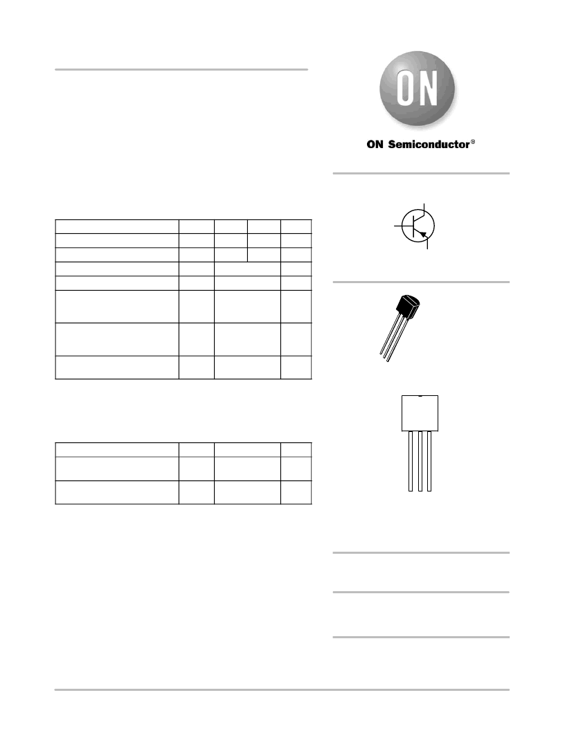
2N
540x
AYWW
A
Y
WW
= Assembly Location
= Year
= Work Week
= PbFree Package
(Note: Microdot may be in either location)
MARKING DIAGRAM
TO92
CASE 29
STYLE 1
123
Preferred
devices are recommended choices for future use
and best overall value.
See detailed ordering and shipping information in the package
dimensions section on page 5 of this data sheet.
ORDERING INFORMATION
http://onsemi.com
*For additional information on our PbFree strategy
and soldering details, please download the
ON Semiconductor Soldering and Mounting
Techniques Reference Manual, SOLDERRM/D.
COLLECTOR
3
2
BASE
1
EMITTER
相關(guān)PDF資料 |
PDF描述 |
|---|---|
| 2N5441 | 40-A Silicon Triacs |
| 2N5442 | 40-A Silicon Triacs |
| 2N5443 | 40-A Silicon Triacs |
| 2N5444 | 40-A Silicon Triacs |
| 2N5445 | 40-A Silicon Triacs |
相關(guān)代理商/技術(shù)參數(shù) |
參數(shù)描述 |
|---|---|
| 2N5400 | 制造商:Fairchild Semiconductor Corporation 功能描述:Bipolar Transistor |
| 2N5400/D | 制造商:MOTOROLA 制造商全稱:Motorola, Inc 功能描述:Amplifier Transistor PNP |
| 2N5400_01 | 制造商:FAIRCHILD 制造商全稱:Fairchild Semiconductor 功能描述:PNP General Purpose Amplifier |
| 2N5400_98 | 制造商:KEC 制造商全稱:KEC(Korea Electronics) 功能描述:TO-92 PACKAGE |
| 2N5400_D26Z | 功能描述:兩極晶體管 - BJT PNP Transistor General Purpose RoHS:否 制造商:STMicroelectronics 配置: 晶體管極性:PNP 集電極—基極電壓 VCBO: 集電極—發(fā)射極最大電壓 VCEO:- 40 V 發(fā)射極 - 基極電壓 VEBO:- 6 V 集電極—射極飽和電壓: 最大直流電集電極電流: 增益帶寬產(chǎn)品fT: 直流集電極/Base Gain hfe Min:100 A 最大工作溫度: 安裝風(fēng)格:SMD/SMT 封裝 / 箱體:PowerFLAT 2 x 2 |
發(fā)布緊急采購(gòu),3分鐘左右您將得到回復(fù)。